Using OpenOCD (Open-On-Chip Debugger) with STM32F411CE: A Practical Guide
Author: Shafeeque Olassery Kunnikkal | Category: IoT, Penetration Testing, STM32F411 | Leave a Comment
Introduction
In this walkthrough, we’ll dive into using OpenOCD to interact with embedded systems via JTAG for debugging and analysis. Our target will be the STM32F411CE microcontroller, specifically the STM32F411CE Lab 3 – Challenge-Response System to understand real-world debugging and firmware application.
This hands-on exercise is designed to introduce real-world IoT pen testing techniques—covering memory access, firmware dumping, and writing data back to the device. Once you’re familiar with these foundational steps, you can apply more advanced bypassing techniques discussed in this article. To further challenge your skills, try testing the methods against these two additional labs:
I hope this hands-on guide provides a solid starting point for your journey into IoT penetration testing.
Prerequisites
Before getting started, make sure you have the following:
- A target microcontroller with JTAG support (e.g., STM32F4 series)
- A compatible JTAG debugger, such as Tigard, ST-Link, or J-Link
- A Linux-based host system, preferably Ubuntu or Debian
- Installed tools:
openocdtelnetgdb-multiarch
- A binary firmware file (
.bin) if you plan to flash the device - Basic familiarity with memory maps and using the terminal
Installing OpenOCD
Option 1: Install via Package Manager
Install OpenOCD using apt:
sudo apt update
sudo apt install openocd
Verify installation:
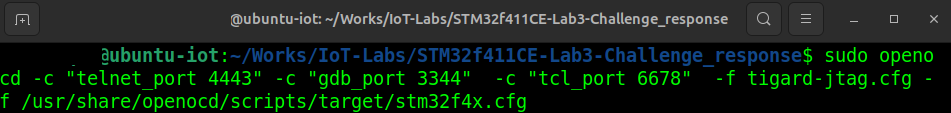
openocd --versionStep 1 – Launch OpenOCD
To get started, initiate OpenOCD — a versatile open-source utility known as the Open-On-Chip Debugger. It allows direct interaction with embedded devices via JTAG and provides essential features such as memory access, firmware flashing, and system data extraction, making it a powerful tool for debugging and analysis.
Run the following command in Terminal 1:
sudo openocd -c "telnet_port 4443" -c "gdb_port 3344" -c "tcl_port 6678" \
-f tigard-jtag.cfg \
-f /usr/share/openocd/scripts/target/stm32f4x.cfg
In the above command:
– The -c flag defines commands to configure OpenOCD.
– We specify custom ports for Telnet, GDB, and TCL.
– The first -f is the Tigard configuration file.
– The second -f is the STM32F4 target configuration file.
Here’s what it looks like in the terminal:
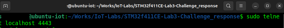
Step 2 – Open a Telnet Session
Open a Telnet session in another terminal (Terminal 2):
sudo telnet localhost 4443Here’s how the command looks in the terminal:
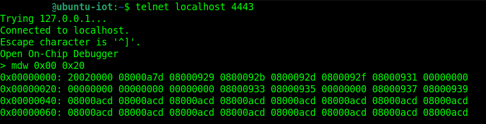
Step 3 – Reading Memory Contents
Once connected via Telnet, one of the first things to test is whether we can read the memory from the device. Use the mdw (memory display word) command to read memory
mdw 0x00 0x20This command reads 0x20 words starting from address 0x00.
Example output:
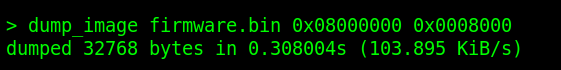
Step 4 – Dumping Firmware
After confirming that we can reliably read memory from the device, the next step is to dump its entire memory contents to a local file. This can be a big win for pen testers, as the dumped data often includes sensitive elements like API keys, encryption keys, URLs, and other valuable variables.
Issue the following commands in Terminal 2:
Reset and halt the target:
reset init
halt
Now check available flash memory banks:
flash banksHere’s how the command looks in the terminal:
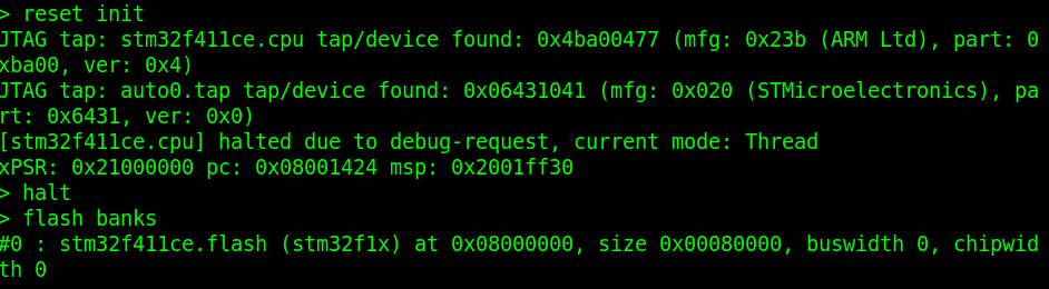
If you are getting flash memory size as zero, refer the trouble shooting section.
Now dump it !.
dump_image firmware.bin 0x08000000 0x00080000This command dumps the contents from 0x08000000 to firmware.bin with a size of 512 KB.
Here’s how the command looks in the terminal:
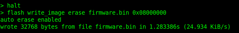
Step 5 – Writing Data to the Device
Writing data can be especially useful when you need to flash entirely new firmware onto an IoT device or modify specific values directly on a real-world target.
You can flash back the dumped firmware like this:
Make sure the target is halted before flashing.
flash write_image erase firmware.bin 0x08000000Here’s how the command looks in the terminal:
Accessing and Modifying Registers
View all registers:
regRead the Program Counter (PC):
reg pcSet a register value (e.g., R0):
reg r0 0xDEADBEEFHalt and set the PC to a new address:
reset halt
reg pc 0x08000000
resume
Troubleshooting: Zero Flash Size in OpenOCD
If you encounter a 0-sized flash bank when using OpenOCD, here are some likely causes and how to fix them.
Likely Causes of Zero Flash Size
1. Incorrect flash driver configuration
The default stm32f4x.cfg includes this line:
flash bank $_FLASHNAME stm32f2x 0 0 0 0 $_TARGETNAMEThe 0 0 means OpenOCD will try to auto-detect the flash base and size.
But if detection fails (e.g., wrong chip ID or unsupported chip), the result is silently a zero-sized flash.
2. Target misidentification
If the $_CPUTAPID doesn’t match the STM32F411CE’s actual JTAG ID (0x4ba00477), OpenOCD may fail during initialization or detect the wrong layout.
3. Flash driver mismatch
Although the STM32F411CE is part of the STM32F4 family, its flash controller behaves like STM32F2 — so:
The correct driver is: stm32f2x
Avoid: stm32f1x, stm32f4x (older OpenOCD versions may not support it properly)
How to Fix It
Replace the auto-detection line with an explicit flash bank declaration:
0x08000000: Start of flash0x80000: 512 KB
This ensures OpenOCD uses the correct memory layout for STM32F411CE.
flash bank $_FLASHNAME stm32f2x 0x08000000 0x80000 0 0 $_TARGETNAMEThe STM32F411CE has 512 KB (0x80000) of flash starting at address 0x08000000.
Appendix: Flash Bank Layout for STM32F411CE
The STM32F411CE microcontroller features a total of 512 KB (0x80000) of Flash memory starting at address 0x08000000. It is organized into multiple sectors that can be individually erased or written.
Flash Sector Map (Main Flash)
| Sector Number | Start Address | Size | Description |
|---|---|---|---|
| Sector 0 | 0x08000000 | 16 KB | Used for boot or config |
| Sector 1 | 0x08004000 | 16 KB | Application/data |
| Sector 2 | 0x08008000 | 16 KB | Application/data |
| Sector 3 | 0x0800C000 | 16 KB | Application/data |
| Sector 4 | 0x08010000 | 64 KB | Main firmware area |
| Sector 5 | 0x08020000 | 128 KB | Main firmware/data |
| Sector 6 | 0x08040000 | 128 KB | Main firmware/data |
| Sector 7 | 0x08060000 | 128 KB | Main firmware/data |
Note: Sectors must be erased before rewriting, and erasing is done per sector.
You can view and verify flash bank info in OpenOCD via:
flash banksAnd list sectors:
flash info 0This layout is critical when selectively dumping, erasing, or flashing specific firmware segments during exploitation or recovery operations.
Final Notes
- Use tools like Binwalk, Strings, and Ghidra to analyze dumped firmware.
- Always verify memory ranges and firmware size before flashing.
- This process is useful not only in development, but also in penetration testing and reverse engineering.